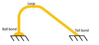
Ball bonding is a type of wire bonding, and is the most common way to make the electrical interconnections between a bare silicon die and the lead frame of the package it is placed in during semiconductor device fabrication.
Gold or copper wire can be used, though gold is more common because its oxide is not as problematic in making a weld. If copper wire is used, nitrogen must be used as a cover gas to prevent the copper oxides from forming during the wire bonding process. Copper is also harder than gold, which makes damage to the surface of the chip more likely. However copper is cheaper than gold and has superior electrical properties,[1] and so remains a compelling choice.
Almost all modern ball bonding processes use a combination of heat, pressure, and ultrasonic energy to make a weld at each end of the wire. The wire used can be as small as 15 μm in diameter—such that several welds could fit across the width of a human hair.
A person upon first seeing a ball bonder will usually compare its operation to that of a sewing machine. In fact there is a needle-like disposable tool called the capillary, through which the wire is fed. A high-voltage electric charge is applied to the wire. This melts the wire at the tip of the capillary. The tip of the wire forms into a ball because of the surface tension of the molten metal.


The ball quickly solidifies, and the capillary is lowered to the surface of the chip, which is typically heated to at least 125 °C. The machine then pushes down on the capillary and applies ultrasonic energy with an attached transducer. The combined heat, pressure, and ultrasonic energy create a weld between the copper or gold ball and the surface of the chip—which is usually copper or aluminum. This is the so-called ball bond that gives the process its name.[2] (All-aluminum systems in semiconductor fabrication eliminate the "purple plague"—a brittle gold-aluminum intermetallic compound—sometimes associated with pure gold bonding wire. This property makes aluminum ideal for ultrasonic bonding.)

Next the wire is passed out through the capillary and the machine moves over a few millimeters to the location that the chip needs to be wired up to (usually called the leadframe[3]). The machine again descends to the surface, this time without making a ball so that the wire is crushed between the leadframe and the tip of the capillary. This time the surface is usually gold, palladium, or silver—but the weld is made in the same way. The resulting weld is quite different in appearance from the ball bond, and is referred to as the wedge bond, tail bond, or simply as the second bond.
In the final step the machine pays out a small length of wire and tears the wire from the surface using a set of clamps. This leaves a small tail of wire hanging from the end of the capillary. The cycle then starts again with the high-voltage electric charge being applied to this tail.
The process where wire is cut right after ball is formed is also called stud bumping. Stud bumping is used when stacking chips in system in package (SIP) modules.[4]
The current state-of-the-art machines (as of 2003[update]) can repeat this cycle about 20 times per second. A modern ball bonder is fully automatic and is essentially a self-sufficient industrial robot, complete with a vision system, sensors, and complex servo systems.
- ^ "Copper (Cu) Wire Bonding or Copper Wirebonding". www.siliconfareast.com.
- ^ "AMETEK Electronic Components and Packaging, a world leading producer of end to end electronic packaging solutions for harsh environments and reliability sensitive applications". www.coininginc.com. Archived from the original on 2014-03-20. Retrieved 2009-07-28.
- ^ "Lead Frames or Leadframes - Page 1 of 2". www.siliconfareast.com.
- ^ "AMETEK Electronic Components and Packaging, a world leading producer of end to end electronic packaging solutions for harsh environments and reliability sensitive applications". www.coininginc.com. Archived from the original on 2010-10-23. Retrieved 2009-07-28.