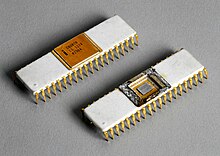
 Closed and open Intel 8080 processor | |
| General information | |
|---|---|
| Launched | April 1974 |
| Discontinued | 1990[1] |
| Marketed by | Intel |
| Designed by | Intel |
| Common manufacturer |
|
| Performance | |
| Max. CPU clock rate | 2 MHz to 3.125 MHz |
| Data width | 8 bits |
| Address width | 16 bits |
| Architecture and classification | |
| Technology node | 6 μm |
| Instruction set | 8080 |
| Physical specifications | |
| Transistors |
|
| Cores |
|
| Package |
|
| Socket | |
| History | |
| Predecessor | Intel 8008 |
| Successor | Intel 8085 |
| Support status | |
| Unsupported | |
The Intel 8080 ("eighty-eighty") is the second 8-bit microprocessor designed and manufactured by Intel. It first appeared in April 1974 and is an extended and enhanced variant of the earlier 8008 design, although without binary compatibility.[3] Although earlier microprocessors were commonly used in mass-produced devices such as calculators, cash registers, computer terminals, industrial robots,[4] and other applications, the 8080 saw greater success in a wider set of applications, and is largely credited with starting the microcomputer industry.[5]
Several factors contributed to its popularity: its 40-pin package made it easier to interface than the 18-pin 8008, and also made its data bus more efficient; its NMOS implementation gave it faster transistors than those of the P-type metal–oxide–semiconductor logic (PMOS) 8008, while also simplifying interfacing by making it TTL-compatible; a wider variety of support chips were available; its instruction set was enhanced over the 8008;[6] and its full 16-bit address bus (versus the 14-bit one of the 8008) enabled it to access 64 KB of memory, four times more than the 8008's range of 16 KB.
It was used in the Altair 8800 and subsequent S-100 bus personal computers until it was replaced by the Z80 in this role, and was the original target CPU for CP/M operating systems developed by Gary Kildall.
The 8080 directly influenced the later x86 architecture. Intel designed the 8086 to have its assembly language be similar enough to the 8080, with most instructions mapping directly onto each other, that transpiled 8080 assembly code could be executed on the 8086.[7]
The initial specified clock rate or frequency limit was 2 MHz, with common instructions using 4, 5, 7, 10, or 11 clock cycles. As a result, the processor is able to execute several hundred thousand instructions per second. Two faster variants, the 8080A-1 and 8080A-2, became available later with clock frequency limits of 3.125 MHz and 2.63 MHz respectively.[8] The 8080 needs two support chips to function in most applications: the i8224 clock generator/driver and the i8228 bus controller. The 8080 is implemented in N-type metal–oxide–semiconductor logic (NMOS) using non-saturated enhancement mode transistors as loads[9][10] thus demanding a +12 V and a −5 V voltage in addition to the main transistor–transistor logic (TTL) compatible +5 V.
- ^ "CPU History – The CPU Museum – Life Cycle of the CPU". Archived from the original on January 16, 2010.
- ^ Lewnes, Ann, "The Intel386 Architecture Here to Stay", Intel Corporation, Microcomputer Solutions, July/August 1989, page 2
- ^ "From CPU to software, the 8080 Microcomputer is here". Electronic News. New York: Fairchild Publications. April 15, 1974. pp. 44–45. Electronic News was a weekly trade newspaper. The same advertisement appeared in the May 2, 1974, issue of Electronics magazine.
- ^ The 8008 (1972) was used for interpolation and control in ASEA's (now ABB) first line of general industrial robots, introduced October 1973.
- ^ Mueller, Scott (2006). Upgrading and Repairing PCs (17th ed.). Pearson Education. p. 37. ISBN 978-0-7897-3404-4. Archived from the original on November 16, 2021. Retrieved November 16, 2021.
- ^ The enhancements were largely based on customer feedback and Federico Faggin and others listening to minicomputer-oriented professionals about certain problems and lack of features in the 8008 architecture. (Source: 8008 and 8080 oral histories.)
- ^ Mazor, Stanley (June 1978). "The Intel 8086 Microprocessor: a 16-bit Evolution of the 8080". IEEE Computer. 11 (6): 18–27. doi:10.1109/C-M.1978.218219. S2CID 16962774. Archived from the original on September 19, 2021. Retrieved November 18, 2021.
- ^ "8080A/8080A-1/8080A-2 8-Bit N Channel Microprocessor" (PDF). Intel. Archived (PDF) from the original on November 15, 2021. Retrieved November 16, 2021.
- ^ similar to pull-up resistors
- ^ Tohya, Hirokazu (2013). Switching Mode Circuit Analysis and Design: Innovative Methodology by Novel Solitary Electromagnetic Wave Theory. Bentham Science Publishers. p. 4. ISBN 9781608054497. Archived from the original on November 15, 2021. Retrieved November 28, 2020.