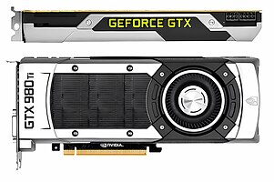
 NVIDIA GeForce GTX 980ti of the GeForce 900-line of graphics-cards, was the final major iteration featuring the Maxwell microarchitecture (GM200-310). | |
| Release date | February 2014 |
|---|---|
| Fabrication process | TSMC 28 nm, 20 nm, 16 nm |
| History | |
| Predecessor | Kepler |
| Successor | Pascal |
| Support status | |
| Supported | |

Maxwell is the codename for a GPU microarchitecture developed by Nvidia as the successor to the Kepler microarchitecture. The Maxwell architecture was introduced in later models of the GeForce 700 series and is also used in the GeForce 800M series, GeForce 900 series, and Quadro Mxxx series, as well as some Jetson products.
The first Maxwell-based products were the GeForce GTX 745 (OEM), GeForce GTX 750, and the GeForce GTX 750 Ti. Both were released on February 18, 2014, both with the chip code number GM107. Earlier GeForce 700 series GPUs had used Kepler chips with the code numbers GK1xx. First-generation Maxwell GPUs (code numbers GM10x) are also used in the GeForce 800M series and the Quadro Kxxx series. A second generation of Maxwell-based products was introduced on September 18, 2014 with the GeForce GTX 970 and GeForce GTX 980, followed by the GeForce GTX 960 on January 22, 2015, the GeForce GTX Titan X on March 17, 2015, and the GeForce GTX 980 Ti on June 1, 2015. The final and lowest spec Maxwell 2.0 card was the GTX950 released on Aug 20th, 2015. These GPUs have GM20x chip code numbers.
Maxwell introduced an improved Streaming Multiprocessor (SM) design that increased power efficiency,[1] the sixth and seventh generation PureVideo HD, and CUDA Compute Capability 5.2.
The architecture is named after James Clerk Maxwell, the founder of the theory of electromagnetic radiation.
The Maxwell architecture is used in the system on a chip (SOC), mobile application processor, Tegra X1.