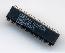

Programmable Array Logic (PAL) is a family of programmable logic device semiconductors used to implement logic functions in digital circuits that was introduced by Monolithic Memories, Inc. (MMI) in March 1978.[1] MMI obtained a registered trademark on the term PAL for use in "Programmable Semiconductor Logic Circuits". The trademark is currently held by Lattice Semiconductor.[2]
PAL devices consisted of a small PROM (programmable read-only memory) core and additional output logic used to implement particular desired logic functions with few components.
Using specialized machines, PAL devices were "field-programmable". PALs were available in several variants:
- "One-time programmable" (OTP) devices could not be updated and reused after initial programming. (MMI also offered a similar family called HAL, or "hard array logic", which were like PAL devices except that they were mask-programmed at the factory.)
- UV erasable versions (e.g.: PALCxxxxx e.g.: PALC22V10) had a quartz window over the chip die and could be erased for re-use with an ultraviolet light source just like an EPROM.
- Later versions (PALCExxx e.g.: PALCE22V10) were flash erasable devices.
In most applications, electrically erasable GALs are now deployed as pin-compatible direct replacements for one-time programmable PALs.
- ^ "Monolithic Memories announces: a revolution in logic design". Electronic Design. 26 (6). Rochelle, NJ: Hayden Publishing: 148B, 148C. March 18, 1978. Introductory advertisement on PAL (Programmable Array Logic).
- ^ Monolithic Memories, Inc (MMI) filed for a work mark on the term "PAL" for use in "Programmable Semiconductor Logic Circuits" on April 13, 1978. A registered trademark was granted on April 29, 1980, registration number 1134025. MMI's first use of the term PAL in commerce was on February 21, 1978. The trademark is currently held by Lattice Semiconductor Corporation of Hillsboro, Oregon. Source: United States Patent and Trademark Office online database.