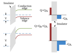
In physics, the field effect refers to the modulation of the electrical conductivity of a material by the application of an external electric field.
In a metal, the electron density that responds to applied fields is so large that an external electric field can penetrate only a very short distance into the material. However, in a semiconductor the lower density of electrons (and possibly holes) that can respond to an applied field is sufficiently small that the field can penetrate quite far into the material. This field penetration alters the conductivity of the semiconductor near its surface, and is called the field effect. The field effect underlies the operation of the Schottky diode and of field-effect transistors, notably the MOSFET, the JFET and the MESFET.[1]
- ^ The acronyms stand for Metal Oxide Semiconductor Field Effect Transistor, Junction Field Effect Transistor, and MEtal Semiconductor Field Effect Transistor. For a discussion see, for example, M K Achuthan K N Bhat (2007). "Chapter 10: Metal semiconductor contacts: Metal semiconductor and junction field effect transistors". Fundamentals of semiconductor devices. Tata McGraw-Hill. pp. 475 ff. ISBN 978-0070612204.