| |

| |
| Names | |
|---|---|
| IUPAC name
Gallium nitride
| |
| Other names
gallium(III) nitride
| |
| Identifiers | |
3D model (JSmol)
|
|
| ChemSpider | |
| ECHA InfoCard | 100.042.830 |
PubChem CID
|
|
| UNII | |
CompTox Dashboard (EPA)
|
|
| |
| |
| Properties | |
| GaN | |
| Molar mass | 83.730 g/mol[1] |
| Appearance | yellow powder |
| Density | 6.1 g/cm3[1] |
| Melting point | > 1600 °C[1][2] |
| Insoluble[3] | |
| Band gap | 3.4 eV (300 K, direct) |
| Electron mobility | 1500 cm2/(V·s) (300 K)[4] |
| Thermal conductivity | 1.3 W/(cm·K) (300 K)[5] |
Refractive index (nD)
|
2.429 |
| Structure | |
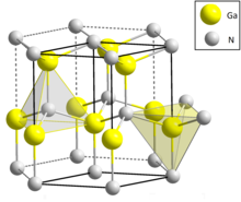
| Wurtzite | |
| C6v4-P63mc | |
a = 3.186 Å, c = 5.186 Å[6]
| |
| Tetrahedral | |
| Thermochemistry | |
Std enthalpy of
formation (ΔfH⦵298) |
−110.2 kJ/mol[7] |
| Hazards | |
| GHS labelling: | |

| |
| Warning | |
| H317 | |
| P261, P272, P280, P302+P352, P321, P333+P313, P501 | |
| NFPA 704 (fire diamond) | |
| Flash point | Non-flammable |
| Safety data sheet (SDS) | Sigma-Aldrich Co., Gallium nitride. Retrieved on 18 February 2024. |
| Related compounds | |
Other anions
|
Gallium phosphide Gallium arsenide Gallium antimonide |
Other cations
|
Boron nitride Aluminium nitride Indium nitride |
Related compounds
|
Aluminium gallium arsenide Indium gallium arsenide Gallium arsenide phosphide Aluminium gallium nitride Indium gallium nitride |
Except where otherwise noted, data are given for materials in their standard state (at 25 °C [77 °F], 100 kPa).
| |
Gallium nitride (GaN) is a binary III/V direct bandgap semiconductor commonly used in blue light-emitting diodes since the 1990s. The compound is a very hard material that has a Wurtzite crystal structure. Its wide band gap of 3.4 eV affords it special properties for applications in optoelectronic,[9][10][11] high-power and high-frequency devices. For example, GaN is the substrate that makes violet (405 nm) laser diodes possible, without requiring nonlinear optical frequency doubling.
Its sensitivity to ionizing radiation is low (like other group III nitrides), making it a suitable material for solar cell arrays for satellites. Military and space applications could also benefit as devices have shown stability in high radiation environments.[12]
Because GaN transistors can operate at much higher temperatures and work at much higher voltages than gallium arsenide (GaAs) transistors, they make ideal power amplifiers at microwave frequencies. In addition, GaN offers promising characteristics for THz devices.[13] Due to high power density and voltage breakdown limits GaN is also emerging as a promising candidate for 5G cellular base station applications. Since the early 2020s, GaN power transistors have come into increasing use in power supplies in electronic equipment, converting AC mains electricity to low-voltage DC.
- ^ a b c Haynes, William M., ed. (2011). CRC Handbook of Chemistry and Physics (92nd ed.). Boca Raton, FL: CRC Press. p. 4.64. ISBN 1-4398-5511-0.
- ^ Harafuji, Kenji; Tsuchiya, Taku; Kawamura, Katsuyuki (2004). "Molecular dynamics simulation for evaluating melting point of wurtzite-type GaN crystal". Journal of Applied Physics. 96 (5): 2501. Bibcode:2004JAP....96.2501H. doi:10.1063/1.1772878.
- ^ Foster, Corey M.; Collazo, Ramon; Sitar, Zlatko; Ivanisevic, Albena (2013). "abstract NCSU study: Aqueous Stability of Ga- and N-Polar Gallium Nitride". Langmuir. 29 (1): 216–220. doi:10.1021/la304039n. PMID 23227805.
- ^ Johan Strydom; Michael de Rooij; David Reusch; Alex Lidow (2019). GaN Transistors for efficient power conversion (3 ed.). California, USA: Wiley. p. 3. ISBN 978-1-119-59442-0.
- ^ Mion, Christian (2005). "Investigation of the Thermal Properties of Gallium Nitride Using the Three Omega Technique", Thesis, North Carolina State University.
- ^ Bougrov V., Levinshtein M.E., Rumyantsev S.L., Zubrilov A., in Properties of Advanced Semiconductor Materials GaN, AlN, InN, BN, SiC, SiGe. Eds. Levinshtein M.E., Rumyantsev S.L., Shur M.S., John Wiley & Sons, Inc., New York, 2001, 1–30
- ^ Haynes, William M., ed. (2011). CRC Handbook of Chemistry and Physics (92nd ed.). Boca Raton, FL: CRC Press. p. 5.12. ISBN 1-4398-5511-0.
- ^ "Safety Data Sheet". fishersci.com. Thermo Fisher Science. 2020. Retrieved 18 February 2024.
- ^ Czelej, K. (2024). "Atomistic Origins of Various Luminescent Centers and n-Type Conductivity in GaN: Exploring the Point Defects Induced by Cr, Mn, and O through an Ab Initio Thermodynamic Approach". Chemistry of Materials. 36 (13): 6392–6409. doi:10.1021/acs.chemmater.4c00178. PMC 11238542.
- ^ Di Carlo, A. (2001). "Tuning Optical Properties of GaN-Based Nanostructures by Charge Screening". Physica Status Solidi A. 183 (1): 81–85. Bibcode:2001PSSAR.183...81D. doi:10.1002/1521-396X(200101)183:1<81::AID-PSSA81>3.0.CO;2-N.
- ^ Arakawa, Y. (2002). "Progress in GaN-based quantum dots for optoelectronics applications". IEEE Journal of Selected Topics in Quantum Electronics. 8 (4): 823–832. Bibcode:2002IJSTQ...8..823A. doi:10.1109/JSTQE.2002.801675.
- ^ Lidow, Alexander; Witcher, J. Brandon; Smalley, Ken (March 2011). "Enhancement Mode Gallium Nitride (eGaN) FET Characteristics under Long Term Stress" (PDF). GOMAC Tech Conference.
- ^ Ahi, Kiarash (September 2017). "Review of GaN-based devices for terahertz operation". Optical Engineering. 56 (9): 090901. Bibcode:2017OptEn..56i0901A. doi:10.1117/1.OE.56.9.090901 – via SPIE.
