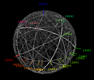
Kikuchi lines are patterns of electrons formed by scattering. They pair up to form bands in electron diffraction from single crystal specimens, there to serve as "roads in orientation-space" for microscopists uncertain of what they are looking at. In transmission electron microscopes, they are easily seen in diffraction from regions of the specimen thick enough for multiple scattering.[1] Unlike diffraction spots, which blink on and off as one tilts the crystal, Kikuchi bands mark orientation space with well-defined intersections (called zones or poles) as well as paths connecting one intersection to the next.
Experimental and theoretical maps of Kikuchi band geometry, as well as their direct-space analogs e.g. bend contours, electron channeling patterns, and fringe visibility maps are increasingly useful tools in electron microscopy of crystalline and nanocrystalline materials.[2] Because each Kikuchi line is associated with Bragg diffraction from one side of a single set of lattice planes, these lines can be labeled with the same Miller or reciprocal-lattice indices that are used to identify individual diffraction spots. Kikuchi band intersections, or zones, on the other hand are indexed with direct-lattice indices i.e. indices which represent integer multiples of the lattice basis vectors a, b and c.
Kikuchi lines are formed in diffraction patterns by diffusely scattered electrons, e.g. as a result of thermal atom vibrations.[3] The main features of their geometry can be deduced from a simple elastic mechanism proposed in 1928 by Seishi Kikuchi,[4] although the dynamical theory of diffuse inelastic scattering is needed to understand them quantitatively.[5]
In x-ray scattering, these lines are referred to as Kossel lines[6] (named after Walther Kossel).
- ^ David B. Williams; C. Barry Carter (1996). Transmission electron microscopy: A textbook for materials science. Plenum Press, NY. ISBN 978-0-306-45324-3.
- ^ K. Saruwatari; J. Akai; Y. Fukumori; N. Ozaki; H. Nagasawa; T. Kogure (2008). "Crystal orientation analyses of biominerals using Kikuchi patterns in TEM". J. Mineral. Petrol. Sci. 103: 16–22. doi:10.2465/jmps.070611.
- ^ Earl J. Kirkland (1998). Advanced computing in electron microscopy. Plenum Press, NY. p. 151. ISBN 978-0-306-45936-8.
- ^ S. Kikuchi (1928). "Diffraction of Cathode Rays by Mica". Japanese Journal of Physics. 5 (3061): 83–96. Bibcode:1928Natur.121.1019N. doi:10.1038/1211019a0.
- ^ P. Hirsch; A. Howie; R. Nicholson; D. W. Pashley; M. J. Whelan (1977). Electron microscopy of thin crystals. Butterworths/Krieger, London/Malabar FL. ISBN 978-0-88275-376-8.
- ^ R. W. James (1982). "Chapter VIII". The Optical Principles of the Diffraction of X-Rays'. Ox Bow Press, Woodbridge, Connecticut. ISBN 978-0-918024-23-7.