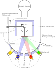
Molecular-beam epitaxy (MBE) is an epitaxy method for thin-film deposition of single crystals. MBE is widely used in the manufacture of semiconductor devices, including transistors.[1] MBE is used to make diodes and MOSFETs (MOS field-effect transistors) at microwave frequencies, and to manufacture the lasers used to read optical discs (such as CDs and DVDs).[2]
- ^ McCray, W.P. (2007). "MBE Deserves a Place in the History Books". Nature Nanotechnology. 2 (5): 259–261. Bibcode:2007NatNa...2..259M. doi:10.1038/nnano.2007.121. PMID 18654274. S2CID 205442147.
- ^ "Alfred Y. Cho". National Inventors Hall of Fame. Retrieved 17 August 2019.