This article needs additional citations for verification. (January 2008) |


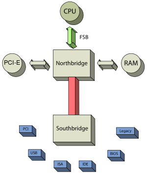
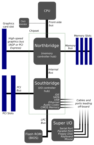
In computing, a northbridge (also host bridge, or memory controller hub) is a microchip that comprises the core logic chipset architecture on motherboards to handle high-performance tasks, especially for older personal computers. It is connected directly to a CPU via the front-side bus (FSB), and is usually used in conjunction with a slower southbridge to manage communication between the CPU and other parts of the motherboard.[1]
Historically, separation of functions between CPU, northbridge, and southbridge chips was necessary due to the difficulty of integrating all components onto a single chip die.[2] However, as CPU speeds increased over time, a bottleneck emerged due to limitations caused by data transmission between the CPU and its support chipset.[3] The trend for integrated northbridges began near the end of the 2000s – for example, the Nvidia GeForce 320M GPU in the 2010 MacBook Air was a northbridge/southbridge/GPU combo chip.[4]
On older Intel based PCs, the northbridge was also named external memory controller hub or graphics and memory controller hub if equipped with integrated graphics. Increasingly these functions became integrated into the CPU chip itself,[5] beginning with memory and graphics controllers. Since the 2010s, die shrink and improved transistor density have allowed for increasing chipset integration, and the functions performed by northbridges are now often incorporated into other components such as southbridges or CPUs themselves.[5][6]
Intel and AMD have both released chipsets in which all northbridge functions had been integrated into the CPU.[6] The corresponding southbridge was renamed by Intel as the Platform Controller Hub and by AMD as the Fusion controller hub. AMD FX CPUs continued to require external northbridge and southbridge chips. Modern Intel Core processors have the northbridge integrated on the CPU die, where it is known as the uncore or system agent.
- ^ "Definition of:Northbridge". PC Magazine. Retrieved September 26, 2015.
- ^ "Chipset: Northbridge and Southbridge". Rigacci.org. 2006-01-27. Retrieved 2015-05-07.
- ^ Kent, Allen (1999). Encyclopedia of computer science and technology. New York, NY [u.a.]: Dekker. p. 500. ISBN 9780824722937. Retrieved September 26, 2015.
- ^ The Macbook Air: A Sign of Things to Come – Digital Gravitas
- ^ a b "Trustworthy x86 laptops? There is a way, says system-level security ace". The Register. Retrieved January 4, 2016.
- ^ a b "Northbridge". Computer Hope. October 7, 2019.