This article needs additional citations for verification. (December 2022) |
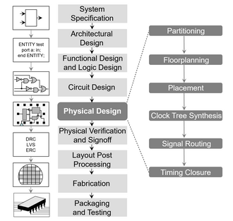
In integrated circuit design, physical design is a step in the standard design cycle which follows after the circuit design. At this step, circuit representations of the components (devices and interconnects) of the design are converted into geometric representations of shapes which, when manufactured in the corresponding layers of materials, will ensure the required functioning of the components. This geometric representation is called integrated circuit layout. This step is usually split into several sub-steps, which include both design and verification and validation of the layout.[1][2]
Modern day Integrated Circuit (IC) design is split up into Front-end Design using HDLs and Back-end Design or Physical Design. The inputs to physical design are (i) a netlist, (ii) library information on the basic devices in the design, and (iii) a technology file containing the manufacturing constraints. Physical design is usually concluded by Layout Post Processing, in which amendments and additions to the chip layout are performed.[3] This is followed by the Fabrication or Manufacturing Process where designs are transferred onto silicon dies which are then packaged into ICs.
Each of the phases mentioned above has design flows associated with them. These design flows lay down the process and guide-lines/framework for that phase. The physical design flow uses the technology libraries that are provided by the fabrication houses. These technology files provide information regarding the type of silicon wafer used, the standard-cells used, the layout rules (like DRC in VLSI), etc.

- ^ N. Sherwani, "Algorithms for VLSI Physical Design Automation", Kluwer (1998), ISBN 9780792383932
- ^ A. Kahng, J. Lienig, I. Markov, J. Hu: "VLSI Physical Design: From Graph Partitioning to Timing Closure", Springer (2022), doi:10.1007/978-90-481-9591-6, ISBN 978-3-030-96414-6, pp. 6-10.
- ^ J. Lienig, J. Scheible (2020). "Chap. 3.3: Mask Data: Layout Post Processing". Fundamentals of Layout Design for Electronic Circuits. Springer. p. 102-110. doi:10.1007/978-3-030-39284-0. ISBN 978-3-030-39284-0. S2CID 215840278.