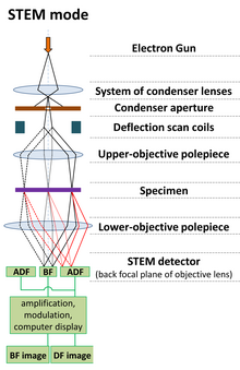


A scanning transmission electron microscope (STEM) is a type of transmission electron microscope (TEM). Pronunciation is [stɛm] or [ɛsti:i:ɛm]. As with a conventional transmission electron microscope (CTEM), images are formed by electrons passing through a sufficiently thin specimen. However, unlike CTEM, in STEM the electron beam is focused to a fine spot (with the typical spot size 0.05 – 0.2 nm) which is then scanned over the sample in a raster illumination system constructed so that the sample is illuminated at each point with the beam parallel to the optical axis. The rastering of the beam across the sample makes STEM suitable for analytical techniques such as Z-contrast annular dark-field imaging, and spectroscopic mapping by energy dispersive X-ray (EDX) spectroscopy, or electron energy loss spectroscopy (EELS). These signals can be obtained simultaneously, allowing direct correlation of images and spectroscopic data.
A typical STEM is a conventional transmission electron microscope equipped with additional scanning coils, detectors, and necessary circuitry, which allows it to switch between operating as a STEM, or a CTEM; however, dedicated STEMs are also manufactured.
High-resolution scanning transmission electron microscopes require exceptionally stable room environments. In order to obtain atomic resolution images in STEM, the level of vibration, temperature fluctuations, electromagnetic waves, and acoustic waves must be limited in the room housing the microscope.[1]
- ^ Muller, D.A.; Grazul, J. (2001). "Optimizing the environment for sub-0.2 nm scanning transmission electron microscopy". Journal of Electron Microscopy. 50 (3): 219–226. doi:10.1093/jmicro/50.3.219. PMID 11469410.