 | |
| Release date | 1998 |
|---|---|
| Designed by | Intel |
| Type | PGA-ZIF |
| Chip form factors | Plastic pin grid array (PPGA) and Flip-chip pin grid array (FC-PGA and FC-PGA2) |
| Contacts | 370[1] |
| FSB protocol | AGTL+, AGTL |
| FSB frequency | 66, 100 and 133 MT/s |
| Voltage range | 1.05–2.1 V |
| Processor dimensions | 1.95 × 1.95 inches[2] (49.53 mm x 49.53 mm) |
| Processors | Intel Celeron Mendocino (PPGA, 300–533 MHz, 2.0 V) Intel Celeron Coppermine (FC-PGA, 533–1100 MHz, 1.5–1.75 V) |
| Predecessor | Slot 1 |
| Successor | Socket 423 |
This article is part of the CPU socket series | |
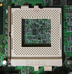
Socket 370, also known as PGA370, is a CPU socket first used by Intel for Pentium III and Celeron processors to first complement and later replace the older Slot 1 CPU interface on personal computers. The "370" refers to the number of pin holes in the socket for CPU pins.
Socket 370 was replaced by Socket 423 in 2000.
- ^ "CPU Sockets Chart". users.erols.com. Retrieved 2009-04-16.
- ^ "Intel Pentium III Specifications" (PDF).