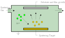
Sputter deposition is a physical vapor deposition (PVD) method of thin film deposition by the phenomenon of sputtering. This involves ejecting material from a "target" that is a source onto a "substrate" such as a silicon wafer. Resputtering is re-emission of the deposited material during the deposition process by ion or atom bombardment.[1][2] Sputtered atoms ejected from the target have a wide energy distribution, typically up to tens of eV (100,000 K). The sputtered ions (typically only a small fraction of the ejected particles are ionized — on the order of 1 percent) can ballistically fly from the target in straight lines and impact energetically on the substrates or vacuum chamber (causing resputtering). Alternatively, at higher gas pressures, the ions collide with the gas atoms that act as a moderator and move diffusively, reaching the substrates or vacuum chamber wall and condensing after undergoing a random walk. The entire range from high-energy ballistic impact to low-energy thermalized motion is accessible by changing the background gas pressure. The sputtering gas is often an inert gas such as argon. For efficient momentum transfer, the atomic weight of the sputtering gas should be close to the atomic weight of the target, so for sputtering light elements neon is preferable, while for heavy elements krypton or xenon are used.[3] Reactive gases can also be used to sputter compounds. The compound can be formed on the target surface, in-flight or on the substrate depending on the process parameters. The availability of many parameters that control sputter deposition make it a complex process, but also allow experts a large degree of control over the growth and microstructure of the film.
- ^ Gregoire, J. M.; Lobovsky, M. B.; Heinz, M. F.; DiSalvo, F. J.; van Dover, R. B. (26 November 2007). "Resputtering phenomena and determination of composition in codeposited films". Physical Review B. 76 (19): 195437. Bibcode:2007PhRvB..76s5437G. doi:10.1103/PhysRevB.76.195437.
- ^ Kester, Daniel J.; Messier, Russell (1 August 1993). "Macro-effects of resputtering due to negative ion bombardment of growing thin films". Journal of Materials Research. 8 (8): 1928–1937. Bibcode:1993JMatR...8.1928K. doi:10.1557/JMR.1993.1928. ISSN 2044-5326. S2CID 221977398.
- ^ Tong, Xingcun Colin (2014). PhD. Schaumburg, IL: Springer International Publishing. p. 42. ISBN 978-3-319-01549-1.