 | |
| Launched | September 20, 2018 |
|---|---|
| Designed by | Nvidia |
| Manufactured by | |
| Fabrication process | TSMC 12FFC |
| Codename(s) | TU10x TU11x |
| Product Series | |
| Desktop | |
| Professional/workstation | |
| Server/datacenter | |
| Specifications | |
| Compute |
|
| L1 cache | 96 KB (per SM) |
| L2 cache | 2 MB to 6 MB |
| Memory support | GDDR6 HBM2 |
| PCIe support | PCIe 3.0 |
| Supported Graphics APIs | |
| DirectX | DirectX 12 Ultimate (Feature Level 12_2) |
| Direct3D | Direct3D 12.0 |
| Shader Model | Shader Model 6.7 |
| OpenCL | OpenCL 3.0 |
| OpenGL | OpenGL 4.6 |
| CUDA | Compute Capability 7.5 |
| Vulkan | Vulkan 1.3 |
| Media Engine | |
| Encode codecs | |
| Decode codecs | |
| Color bit-depth |
|
| Encoder(s) supported | NVENC |
| Display outputs | |
| History | |
| Predecessor | Pascal |
| Variant | Volta (datacenter/HPC) |
| Successor | Ampere |
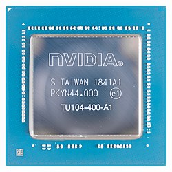
Turing is the codename for a graphics processing unit (GPU) microarchitecture developed by Nvidia. It is named after the prominent mathematician and computer scientist Alan Turing. The architecture was first introduced in August 2018 at SIGGRAPH 2018 in the workstation-oriented Quadro RTX cards,[2] and one week later at Gamescom in consumer GeForce 20 series graphics cards.[3] Building on the preliminary work of Volta, its HPC-exclusive predecessor, the Turing architecture introduces the first consumer products capable of real-time ray tracing, a longstanding goal of the computer graphics industry. Key elements include dedicated artificial intelligence processors ("Tensor cores") and dedicated ray tracing processors ("RT cores"). Turing leverages DXR, OptiX, and Vulkan for access to ray tracing. In February 2019, Nvidia released the GeForce 16 series GPUs, which utilizes the new Turing design but lacks the RT and Tensor cores.
Turing is manufactured using TSMC's 12 nm FinFET semiconductor fabrication process. The high-end TU102 GPU includes 18.6 billion transistors fabricated using this process.[1] Turing also uses GDDR6 memory from Samsung Electronics, and previously Micron Technology.
- ^ a b "Nvidia Turing GPU Architecture: Graphics Reinvented" (PDF). Nvidia. 2018. Retrieved June 28, 2019.
- ^ Smith, Ryan (August 13, 2018). "NVIDIA Reveals Next-Gen Turing GPU Architecture: NVIDIA Doubles-Down on Ray Tracing, GDDR6, & More". AnandTech. Retrieved April 9, 2023.
- ^ Smith, Ryan (August 20, 2018). "NVIDIA Announces the GeForce RTX 20 Series: RTX 2080 Ti & 2080 on Sept. 20th, RTX 2070 in October". AnandTech. Retrieved April 9, 2023.